Design a Memory System Using Four Memory Chips
- The processor can usually address a memory space that is much larger than the memory space covered by an individual memory chip.
- In order to splice a memory device into the address space of the processor, decoding is necessary.
- For example, the 8088 issues 20-bit addresses for a total of 1MB of memory address space.
- However, the BIOS on a 2716 EPROM has only 2KB of memory and 11 address pins.
- A decoder can be used to decode the additional 9 address pins and allow the EPROM to be placed in any 2KB section of the 1MB address space.
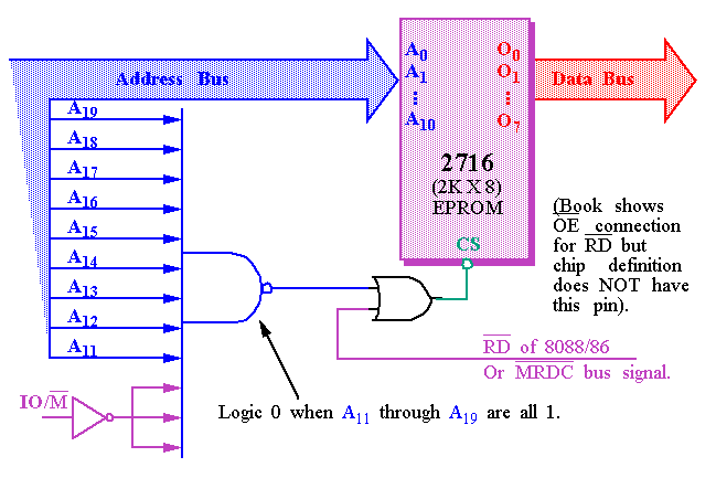
- To determine the address range that a device is mapped into:
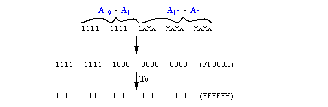
- This 2KB memory segment maps into the reset location of the 8086/8088 (FFFF0H).
- NAND gate decoders are not often used.
- Rather the 3-to-8 Line Decoder (74LS138) is more common.
- The 3-to-8 Line Decoder (74LS138)
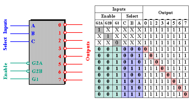
- Note that all three Enables (G2A, G2B, and G1) must be active, e.g. low, low and high, respectively.
- Each output of the decoder can be attached to an 2764 EPROM ( 8K X 8 ).
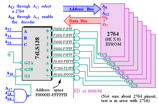
- The EPROMs cover a 64KB section of memory.
- Yet a third possibility is a PLD (Programmable Logic Device).
- PLDs come in three varieties:
- PLA (Programmable Logic Array)
- PAL (Programmable Array Logic)
- GAL (Gated Array Logic)
- PLDs have been around since the mid-1970s but have only recently appeared in memory systems (PALs have replaced PROM address decoders).
- PALs and PLAs are fuse-programmed (like the PROM).
- Some are erasable (like the EPROM).
- A PAL example (16L8) is shown in the text and is commonly used to decode the memory address, particularly for 32-bit addresses generated by the 80386DX and above.
- AMD 16L8 PAL decoder.
- It has 10 fixed inputs (Pins 1-9, 11), two fixed outputs (Pins 12 and 19) and 6 pins that can be either (Pins 13-18).

- AND/NOR device with logic expressions (outputs) with up to 16 ANDed inputs and 7 ORed product terms.
- The memory systems "sees" the 8088 as a device with:
- 20 address connections (A19 to A0).
- 8 data bus connections (AD7 to AD0).
- 3 control signals, IO/M, RD, and WR.
- We'll look at interfacing the 8088 with:
- 32K of EPROM (at addresses F8000H through FFFFFH).
- 512K of SRAM (at addresses 00000H through 7FFFFH).
- The EPROM interface uses a 74LS138 (3-to-8 line decoder) plus 8 2732 ( 4K X 8 ) EPROMs.
- The EPROM will also require the generation of a wait state.
- The EPROM has an access time of 450ns .
- The 74LS138 requires 12ns to decode.
- The 8088 runs at 5MHz and only allows 460ns for memory to access data.
- A wait state adds 200ns of additional time.

- The 8088 cold starts execution at FFFF0H . JMP to F8000H occurs here.
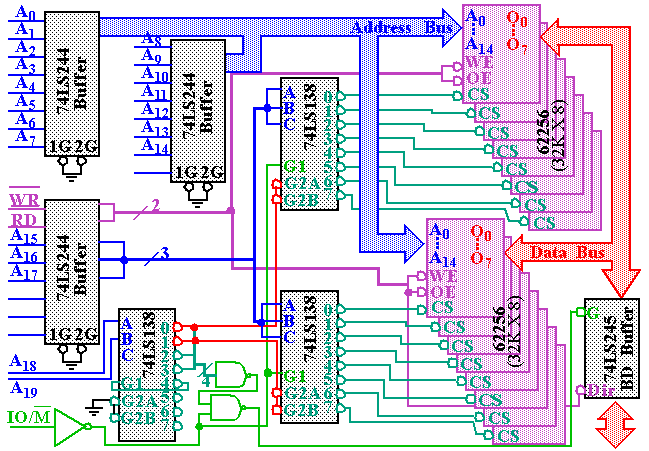
- The 16 62256s on the previous slide are actually SRAMs.
- Access times are on order of 10ns .
- Flash memory can also be interfaced to the 8088 (see text).
- However, the write time ( 400ms !) is too slow to be used as RAM (as shown in the text).
- Parity Checking:
- Parity checking is used to detect single bit errors in the memory.
- The current trend is away from parity checking.
- Parity checking adds 1 bit for every 8 data bits.
- For EVEN parity, the 9th bit is set to yield an even number of 1's in all 9 bits.
- For ODD parity, the 9th bit is set to make this number odd.
- For 72-pin SIMMs, the number of data bits is 32 + 4 = 36 ( 4 parity bits).
- 74AS280 Parity Generator/Checker
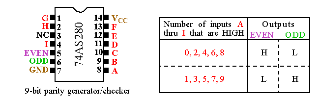
- This circuit generates EVEN or ODD parity for the 9-bit number placed on its inputs.
- Typically, for generation, the 9th input bit is set to 0.
- This circuit also checks EVEN or ODD parity for the 9-bit number.
- In this case, the 9th input bit is connected to the 9th bit of memory.
- For example, if the original byte has an even # of 1's (with 9th bit at GND), the parity bit is set to 1 (from the EVEN output).
- If the EVEN output goes high during the check, then an error occurred.
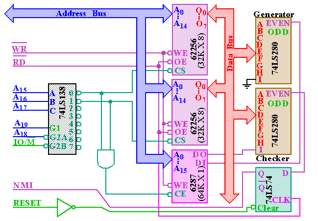
- This parity scheme can only detect a single bit error.
- Block-Check Character ( BCC ) or Checksum.
- Can detect multiple bit errors.
- This is simply the two's complement sum (the negative of the sum) of the sequence of bytes.
- No error occurred if adding the data values and the checksum produces a 0.
- For example:

- This is not fool proof.
- If 45 changes to 44 AND 04 changes to 05, the error is missed.
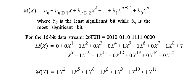
- Cyclic Redundancy Check ( CRC ).
- Commonly used to check data transfers in hardware such as harddrives.
- Treats data as a stream of serial data n-bits long.
- The bits are treated as coefficients of a characteristic polynomial , M(X) of the form:
- Cyclic Redundancy Check ( CRC ) (cont.)
- The CRC is found by applying the following equation.

- G(X) is the called the generator polynomial and has special properties.
- A commonly used polynomial is:

- The remainder R(X) is appended to the data block.
- When the CRC and R(X) is computed by the receiver, R(X) should be zero.
- Since G(X) is of power 16, the remainder, R(X) , cannot be of order higher than 15.
- Therefore, no more than 2 bytes are needed independent of the data block size.
- Cyclic Redundancy Check ( CRC )(cont.)

- Parity , BCC and CRC are only mechanisms for error detection.
- The system is halted if an error is found in memory.
- Error correction is starting to show up in new systems.
- SDRAM has ECC (Error Correction Code).
- Correction will allow the system can continue operating.
- If two errors occur, they can be detected but not corrected .
- Error correction will of course cost more in terms of extra bits.
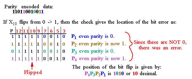
- Error correction is based on Hamming Codes .
- There is lots of theory here but our focus will be on implementation.
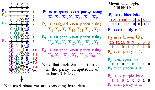
- The objective is to correct any single bit errors in an 8-bit data byte.

- In other words, we need 4 parity bits to correct single bit errors.
- Note that the parity bits are at bit positions that are powers of 2 .
- Hamming Codes (cont).
- P1 is generated by computing the parity of X 3 , X 5 , X 7 , X 9 , X 11 , X 13 , X 15 .
- These numbers have a 1 in bit position 1 of the subscript in binary.
- Hamming Codes (cont).
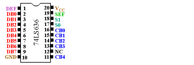
- The 74LS636 corrects errors by storing 5 parity bits with each byte of data.
- The pinout consists of:
- 8 data I/O pins
- 5 check bit I/O pins
- 2 control pins
- 2 error outputs
- Single error flag ( SEF )
- Double error flag ( DEF ).
- See the text for an example of its use in a circuit.
Design a Memory System Using Four Memory Chips
Source: https://ece-research.unm.edu/jimp/310/slides/8086_memory2.html
0 Response to "Design a Memory System Using Four Memory Chips"
Post a Comment